2.2.1. Access memory directly and indirectly
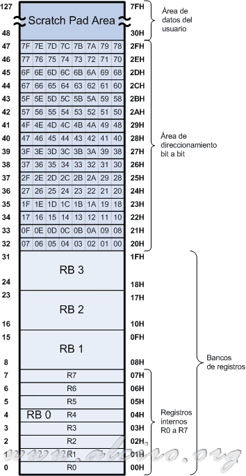
The area of direct and indirect addressing is made up of the first 128 bytes of internal memory of the microcontroller. This in turn is divided into three segments differentiated by their use.

Area of direct and indirect addressing of internal RAM
The register banks.
Internal records or auxiliary accumulator is 8, R0 to R7, its mission is to support the accumulator in their work process. The instruction set of the 8051 microcontroller is targeted directly to work with a single register, the accumulator and a secondary registers R0 to R7.
In turn, the registers R0 to R7 are grouped into 4 banks of registers, RB0 to RB3 that match the top of internal memory, we are occupying positions RB0 00H to 07H, the 08H RB1 to 0FH and so on (see figure below).
You can switch from bank records software work by setting the bits B3 and B4 of the status register PSW. This system is used to safeguard the state of internal registers between different software processes to the CPU, you can switch from bank records when access or returns in a subroutine, to an interrupt request etc.
Address area bit by bit
The address area bit by bit consists of 16 bytes in internal RAM locations 20H to 2Fh. Each byte is divided into 8 bits, with corresponding numbers between 0 and 127 for a total of 128 bits, which can be accessed by addressing specific instructions bit by bit. To refer to a particular bit, you can specify its number or the memory location and the bit in question from 0 to 7. For example, bit 0 is 20.0, 1, 20.1, 9 is 21.0 and so on.
This area also supports the normal address bytes. For example, we can activate the 09H bit by bit instructions.
SETB 09H ; Poner a 1 el bit 9
Or by Bytes handling instructions.
ORL 21H,#00000010B ; Suma lógica (OR) en el Byte 21H el dato inmediato 00000010B
Área Scratch Pad
The Scratch Pad memory area or fast access memory called Notepad is located in the internal RAM location 30H to 7FH. It is intended to work with data as the user's working memory, is more agile than the external RAM to the microcontroller, but while the external RAM can have a sufficient capacity for any application (64KB), the Scratch Pad area is limited to 96 Bytes.
Barring external RAM (XRAM), the storage capacity of these microcontrollers is very limited, 96 Bytes 128 Bytes Scratch Pad memory more accessible only indirectly.


